Our revolutionary material heralds a new era for light emitting devices, a technology that brings cutting-edge advantages to LEDs, microLEDs, displays and a host of end-user products.
We address a range of applications, using our platform material technology, to bring significant customer benefits and enhance the end-user’s experience.
Displays
Delivering a native red microLED and improved green efficiency for applications such as AR/VR and TVs.
General lighting
Bridging the ‘green gap’ to enable high efficiency, colour mixed, white solid state lighting.
Visible Light Communications
Improving switching speeds and higher efficiencies, to enhance applications such as fibre optics and LiFi.
Our Cubic GaN Technology
Kubos has developed the first commercially compatible Cubic GaN growth process enabling more efficient long wavelength LEDs.
Using the cubic crystal phase of GaN we overcome the limitations of conventional GaN LEDs allowing us to ultimately deliver significantly higher efficiency green, amber and red devices.
- Improved efficiency at longer wavelengths
- Fully compatible with standard industry manufacturing equipment and processes
- Scalable to large diameter, volume production
- Kubos’ technology operates more efficiently in the green and amber regions for all LEDs and into the red for microLEDs
- Graph shows efficiency roll-off of conventional LEDs and microLEDs

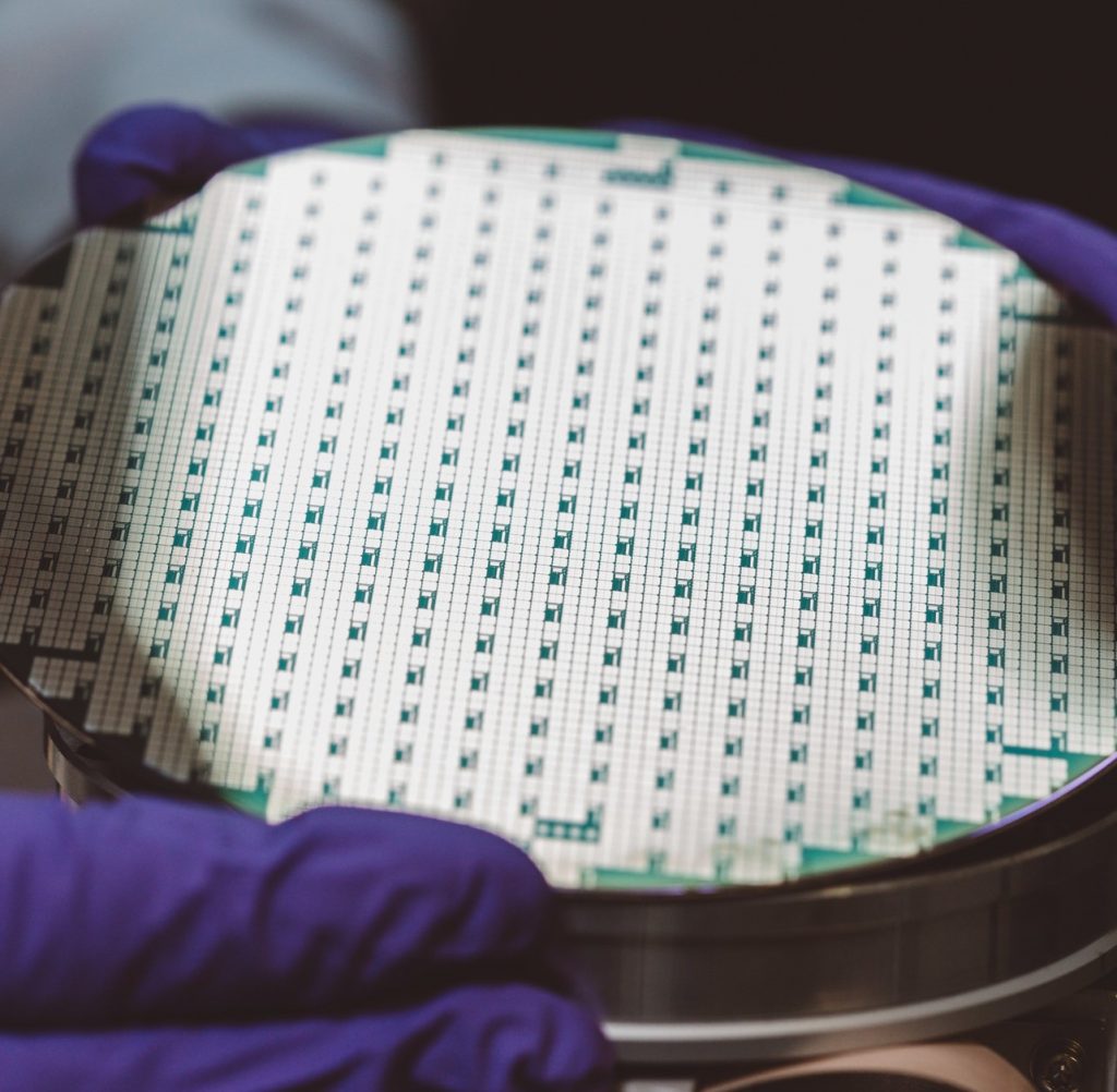
- 150mm (6 “) wafers available – contact us
- Scalable to 200mm (8”) and beyond
- Growth process fully compatible with standard MOCVD production tools
- Low-cost silicon (001) CMOS substrate
- Thin layer of 3c-SiC (standard CVD process)
KubosLED Preliminary Product Brief
Kubos Semiconductors has developed technology to produce efficient, high brightness, full-colour microLED displays. As a result, the patented process technology for this single material system overcomes one of the main roadblocks in the AR/VR headset and the display market.
To achieve world-leading efficiency, Kubos produces device-quality, epitaxial layers of gallium, indium, and aluminium nitride (Group III nitrides) and their alloys in the cubic phase.
Key Benefits for RGB Markets
In one of the first major breakthroughs in light emitting devices, since the early 1990s, our revolutionary material platform delivers significant performance benefits in LED and microLED devices. The beneficiaries of these improvements span a wide range of lighting, display and visible light communications applications. It enables large scale production with low manufacturing costs of high-performance, high-efficiency LEDs.
- Improved low energy consumption
- Fabrication of RGB devices using the same substrate material
- Device process highly compatible with hexagonal-GaN vertical LEDs
- Scalable production established on 150mm Silicon with potential to be transferred to 200mm and beyond
- Reduced current droop
- Increased efficiency
- Reduced spectral drift (blue shift) with drive current
- Faster switching speeds
- Silicon CMOS compatible substrate to support future driver integration
Kubos Cubic Technology Vs standard Hexagonal GaN Technology
| Feature | Cubic GaN | Standard Hex-GaN |
|---|---|---|
| High efficiency achievable (>550nm) | Yes | No |
| QCSE eliminated | Yes | No |
| Indium content (as a function of wavelength) | Low | High |
| Carrier Lifetime | Short | long |
| Colour conversion (QDs) required for Red/Green | No | Yes |
| Droop effect | Low | High |
| Blue shift effect at longer wavelengths | Low | High |
Low Carbon Emissions
Kubos’ LED technology is a significant step towards more efficient solid-state lighting which has the potential to significantly reduce carbon emissions.
Our LEDs could save up to 500M tonnes of CO2 emissions (over 5 years) in lighting and a further 100M tonnes in displays, based on 100% adoption. That’s the equivalent to annual carbon emissions from 150 coal fired power stations.
Our Story
Kubos is developing highly efficient LEDs using our proprietary Cubic GaN technology to improve the user experience for lighting, displays and communications across the visible spectrum. The LED stacks built on our technology can be easily integrated into the pre-existing commercial LED fabrication process, enabling increased efficiency of red and green LEDs at reduced cost.
Formed in 2017 to commercialise the technology first developed in a partnership between the University of Cambridge and Anvil Semiconductors. This partnership built on Anvil’s proprietary device quality silicon carbide on 150 mm diameter silicon wafers to develop a Cubic GaN growth process by MOCVD (metal organic chemical vapour-phase deposition).
Today, Kubos is pioneering advancements in this material technology for LEDs and microLEDs, delivering unique benefits and advantages to the market. Bringing the first step change in performance of LEDs since the first blue LEDs were invented 30 years ago.